The Spintronics Research Center at Keio University performs state-of-the-art Spintronics research.
This site supported by;
Spintronics Research Network of Japan (Spin-RNJ)
JSPS Core-to-Core Program "Isotope Spintronics"
aims to provide a platform for spintronic researchers to collaborate and exchange ideas in order to push the envelope on Spintronics Research.
本サイトは
スピントロニクス学術研究基盤と連携ネットワーク
日本学術振興会拠点形成事業「同位体スピントロニクス」
により運営されています。
以下の スピントロニクス学術連携研究教育センター Center for Spintronics Research Network (CSRN) とともに連携しています。
東北大学 大阪大学 東京大学
Videos
The video menu below shows a list of research videos presented by researchers in the field.
Spintronics Research Videos (Please select topics)
Quantum Information
Review Talk
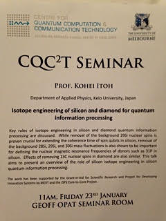
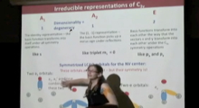
Oct. 2009 by K. M. Itoh, Keio University, on; "Silicon Quantum Processing". [Video]
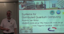
Dec. 2009 by R.V. Meter, Keio University, on; "Systems for Distributed Computing". [Video]
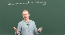
Jan. 2011 by S. Lloyd, Keio University, on; "Quantum algorithm for solving linear equations". [Video]
Jan. 2011 by S. Lloyd, Keio University, on; "photosynthesis - 'Quantum Life'". [Video]
Quantum Information
Oct. 2009 by K.M. Itoh on; H. Hayashi, T. Itahashi, K. M. Itoh, L. S. Vlasenko and M. P. Vlasenko, "Dynamic Nuclear Polarization of 29Si Nuclei in Isotopically Controlled Phosphorus Doped Silicon," Phys. Rev. B 80, 045201 (2009). [Article 1] and "Nuclear Magnetic Resonance Linewidth and Spin Diffusion in 29Si Isotopically Controlled Silicon," Phys. Rev. B 78, 153201 (2008) [Article 2][Video]
Oct. 2009 by T. Arai, Keio University, on; "Scanning Tunneling Microscopy and Spectroscopy of Silicon Atomic Wire,". [Video]
Oct. 2009 by T. Ishikawa, Keio University in collaboration with A.F. loffe Physico-Technical Institute of Russian Academy of Science, on; "Photoluminescence from triplet states of isoelectronic bound excitons at interstitial-carbon-interstitial-oxygen defects in silicon,". [Video]
Oct. 2009 by M.R. Rahman, Keio University, on; "Electron Paramagnetic Resonance and Dynamic Nuclear Polarization of 29Si Nuclei in Lithium-Doped Silicon,". [Video]
Oct. 2009 by W. Akhtar, Keio University, on; "Electrically Detected Magnetic Resonance of Phosphorus in Silicon at Low Magnetic Field,". [Video]
Oct. 2009 by A. Trisetyarso, Keio University, on; "Circuit Design for Measurement-based Quantum Carry Lookahead Adder,". [Video]
Dilute Magnetic Semiconductors
Review Talk
[Article] [Video]
Materials Science and Chemistry
[Article] [Video]
Physics
[Article] [Video]
Non-magnetic Semiconductors
Review Talk
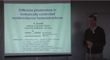
Nov. 2009 by H. Bracht, Institute of Material Physics, University of Münster, Germany, on; "Diffusion Phenomena in Isotopically Controlled Semiconductor Heterostructures". [Video]
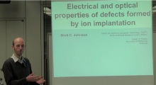
Jan. 2010 by B. Johnson, Centre for Quantum Computer Technology, University of Melbourne, Australia, on; "Electrical and Optical Properties of Defects Formed by Ion Implantation". [Video]
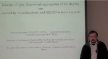
Jan. 2010 by R. Morgunov, Institute of Problems of Chemical Physics, Russian Academy of Sciences, Chernogolovka, Russia, on; Kinetics of spin-dependent aggregation of the doping ions studied by microhardness and SQUID in ionic crystals. [Video]
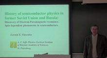
March. 2010 by L.S. Vlasenko, A. F. Ioffe Physico-Techical Institute of Russian Academy of Sciences, St. Petersburg, Russia, on; History of semiconductor physics in former Soviet Union and Russia. [Video]
Jan. 2011 by L.S. Vlasenko, A. F. Ioffe Physico-Techical Institute of Russian Academy of Sciences, St. Petersburg, Russia, on; Spin Dependent Effects in Semiconductors : application to magnetic resonance. [Video]
Aug. 2011 by A. Wray, Lawrence Berkeley National Laboratory , Princeton University , California , USA., on; Electron dynamics in topological insulator based semiconductor-metal interfaces. [Video]
Nov. 2011 by G. Abstreiter , Walter Schottky institut-ZNN , Physik Department and Institute for Advanced Study , Garching , Germany , on; Si/Ge based nanostructures and arsenide based nanowires on Si. [Video]
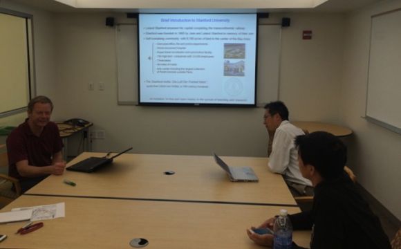
Jan. 2012 by I. Appelbaum , Materials Science and Engineering , College Park, USA , on; Spin Transport in Silicon. [Video]
Jan. 2012 by P.C. McIntyre , Materials Science and Engineering , Stanford University, Stanford , USA , on; Ge Core - Si(Ge) Shell Nanowires : Stability and Surface Passivation. [Video]
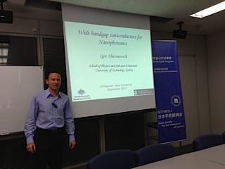
Sep. 2013 by I. Aharonovich , School of Physics and Advanced Materials , University of Technology Sydney, Sydney , Australia, on; Wide band gap semiconductors for Nanophotonics. [Video]
Materials Science and Chemistry
Oct. 2009 by S. Miyamoto, Keio University, on; S. Miyamoto, O. Moutanabbir, E. E. Haller and K. M. Itoh, “Spatial Correlation of Self-Assembled Isotopically Pure Ge/Si(001) Nanoislands,” Phys. Rev. B. 79, 165415 (2009). [Article][Video]
Oct. 2009 by Y. Kawamura, Keio University, on; M. Naganawa, Y. Kawamura, Y. Shimizu, M. Uematsu, K. M. Itoh, H. Ito, M. Nakamura, H. Ishikawa, and Y. Ohji, "Accurate Determination of the Intrinsic Diffusivities of Boron, Phosphorus and Arsenic in Silicon: The Influence of SiO2 Films," Jpn. J. Appl. Phys., 47, 6205 (2008). [Article][Video]
Nov. 2009 by R. Hirano, Keio University, on; "Room-temperature Observation of Quantum Size Effects in Photoluminescence of Si(0.8)GE(0.2)/Si Nanocolumns Prepared by Neutral Beam Etching,".[Video]
Physics
Oct. 2009 by S. Miyamoto, Keio University, on; S. Miyamoto, K. Nishiguchi, Y. Ono, K. M. Itoh, and A. Fujiwara, “Escape Dynamics of a Few Electrons in a Single-Electron Ratchet using Silicon Nanowire Metal-Oxide-Semiconductor Field-Effect Transistor,” Appl. Phys. Lett. 93, 222103 (2008). [Article][Video]
Oct. 2009 by S. Miyamoto, Keio University, on; S. Miyamoto, K. Nishiguchi, Y. Ono, K. M. Itoh, and A. Fujiwara, “Resonant Escape over an Oscillating Barrier in Single-Electron Ratchet Transfer,” submitted to Phys. Rev. B. [Video]
Oct. 2009 by Y. Kawamura, Keio University in collaboration with University of California at Berkeley, on; "Quantitative Evaluation of Germanium Displacement induced by Arsenic Implantation using Germanium Isotope Superlattices". [Video]
Oct. 2009 by T. Ishikawa, Keio University in collaboration with Simon Fraser University and A.F. loffe Physico-Technical Institute of Russian Academy of Science, on; "Photoluminescence Study of Isoelectronic Centers in Silicon - Beryllium Pairs and Carbon-Oxygen Defects,". [Video]
Oct. 2009 by G. Tsuchiya, Keio University, on; "Identification of the Influence of Phonon Scattering on the Electron Mobility in a Strained-Si Quantum Well,". [Video]
Oct. 2009 by H. Tezuka, Keio University, on; "EPR Study of Boron in Silicon: Isotope effect and Double Excitation,". [Video]
Nov. 2009 by K. Naito, Keio University, on; "Photoluminescence of Erbium Doped Isotopically Controlled Silicon,". [Video]
Dec. 2009 by L.J. Garcia, Keio University, on; "Amorphization of Semiconductors,". [Video]
Spin Electronics and Spin Photonics on Oxide Semiconductors - Hitoshi Tabata (University of Tokyo) [Video]
Anisotropic spin transport induced by competition between Rashba and Dresselhaus spin-orbit interactions in InGaAs wires - Junsaku Nitta (Tohoku University) [Video]
Keio Topical Workshop on Semiconductor Spintronics (2013) - English-only
Recent topics in diluted magnetic semiconductors - Hideo Ohno (Tohoku University) [Video]
University of Tokyo, Prof. Yasunobu Nakamura’s seminar room
Speaker
Dr. Hans Huebl
“Nano-opto-mechanics at microwave frequencies”
_______________________________
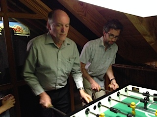
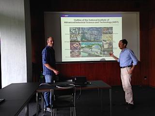
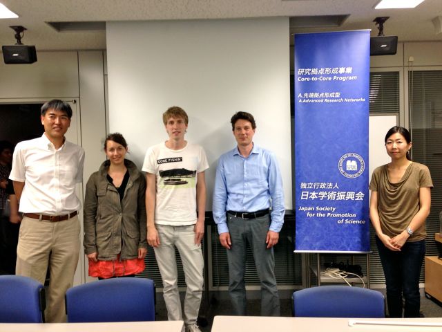
TU Munich-Keio meeting on silicon isotope spintronics
June 7, 2014, 5pm-9pm
TU Munich
Martin Brandt (TUM), Hans Huebl (TUM), Kohei M. Itoh (Keio)
_______________________________
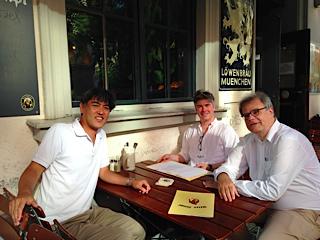
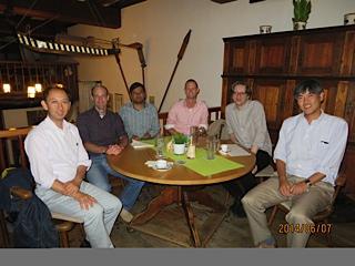
Ulm-ETH Zurich-Keio joint meeting and seminar on diamond quantum sensing
June 6, 2014, 12:00pm-5:30pm
Fedor Jelezko (Ulm), Christian Degen (ETH), Liam McGuinness (ETH),
Phani Peddibhotla (Ulm), Hideyuki Watanabe (AIST), Kohei M. Itoh (Keio)
_______________________________
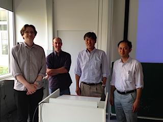
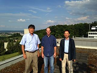
ETH Zurich-Keio joint meeting and seminar on diamond quantum sensing
June 2, 2014, 2:30pm-5:30pm
ETH Zurich, Physics Department, Seminar Room
Christian Degen (ETH), Klaus Ensslin (ETH), Michael Loretz (ETH), Tobias Rosskopt (ETH), Hideyuki Watanabe (AIST), Kohei M. Itoh (Keio)
_______________________________
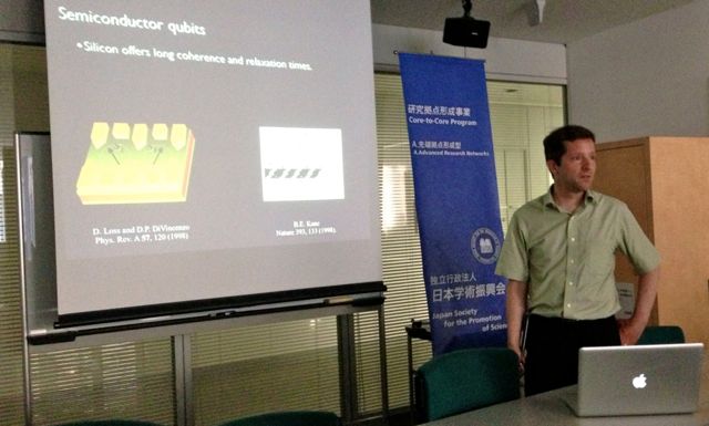
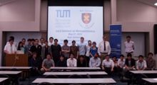
TU Munchen-Keio joint symposium on nanoelectronics 2013
December 16, 2013, 12:30pm-5:30pm
TU Munich, Seminar Room ZNN
Program
13:35 Prof. Junko Hayase (Keio)
"Semiconductor quantum dots optical quantum information processing"
14:00 Prof. Jonathan Finley (TUM)
"All optical coherent spin control in quantum dots and molecules"
14:25 Prof. Hideyuki Maki (Keio)
"Carbon nanotube optoelectronics"
14:50 Prof. Alex Holleitner (TUM)
"Polarization control of ultrafast spin currents in topological insulators"
15:15 Coffee
15:45 Prof. Kazuya Ando (Keio)
"Spin current in metals, insulators, and semiconductors"
16:10 Priv.-Doz. Sebastian Gönnenwein (Bayerische Akademie der Wissenschaften)/li>
"Spin currents in magnetic insulator/normal metal hybrids"
16:35 Prof. Kohei Itoh (Keio)
"Semiconductor isotope spintronics; silicon and diamond quantum information processing and sensing"
17:00 Prof. Martin Brandt (TUM)
"Measuring electric field gradients with spins"
_______________________________
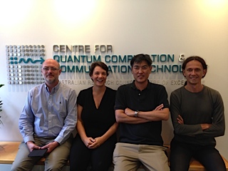
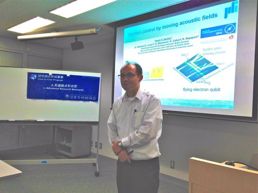
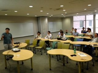
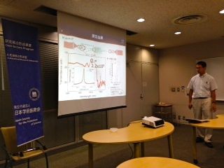
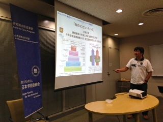
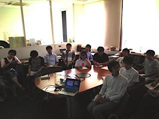
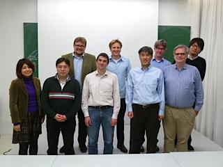
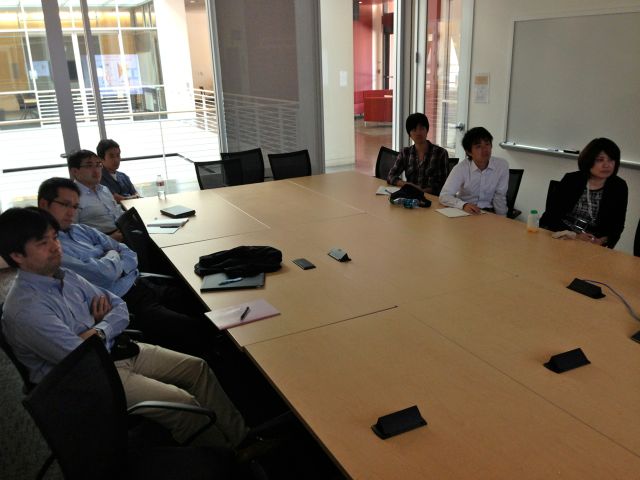
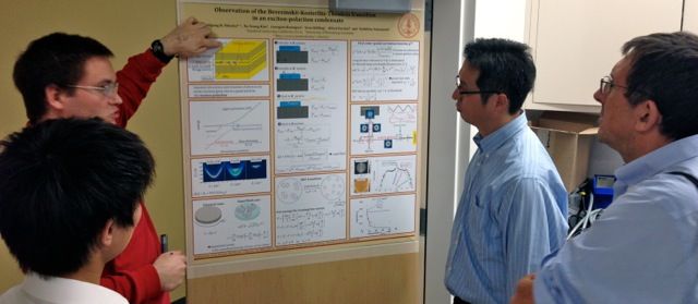
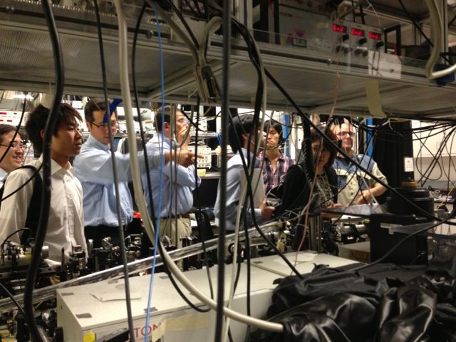
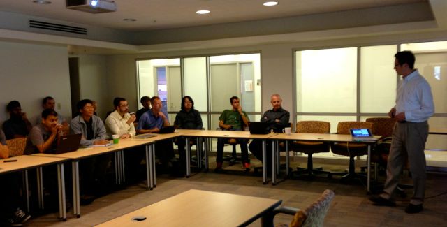
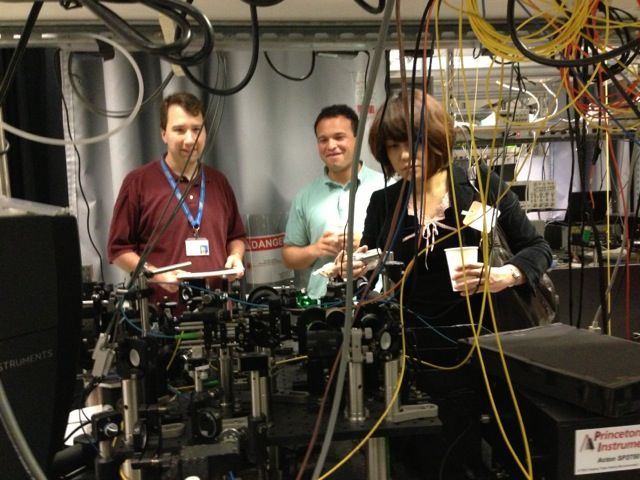
Project Member Meeting
November 27, 2013
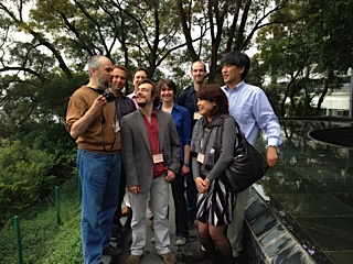
NMR Quantum Information Processing in Rio 2013
From right to left: Prof. Jonathan Baugh (Univ. Waterloo), Kohei Itoh (Keio), Prof. Ivan Santos Oliveira (CBPF), Prof. Raymond Laflamme (Univ. Waterloo), Prof. John Morton (UCL)
_______________________________
Special Seminar on Diamond Spintronics
_______________________________
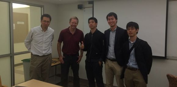
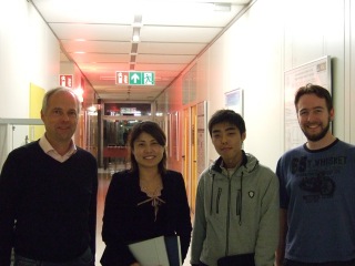
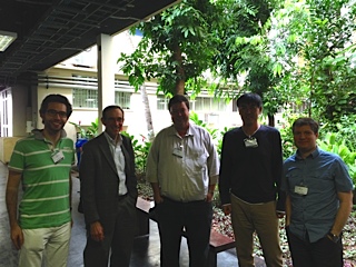
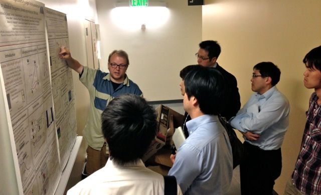
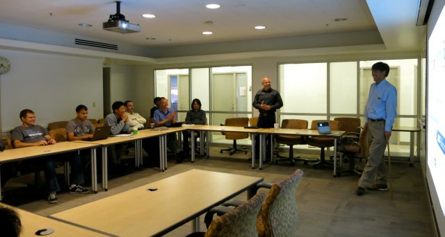
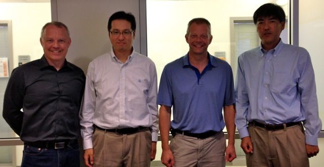
Project Member Meeting
July 22, 2013
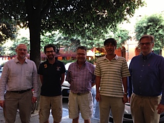
International Conference on Defects in Semiconductors, Bologna, Italy
From right to left: Prof. Martin Brandt (TU Munich), Kohei Itoh (Keio), Prof. Mike Thewalt (Simon Fraser Univ.), Prof. John Morton (UCL), Prof. Sven Rogge (Univ. New South Wales)
_______________________________
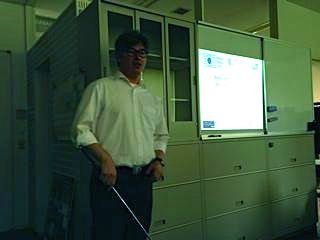
Special Seminar on Si Quantum Information Processing
July 16, 2013
Keio University Yagami Campus, bldg. 14, DR2
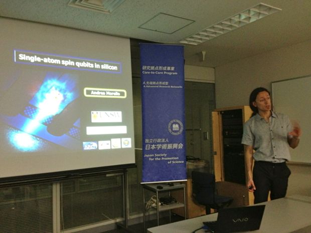
Professor Andrea Morello (University of New South Wales)
"single-atom spin qubits in silicon"
_______________________________
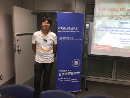
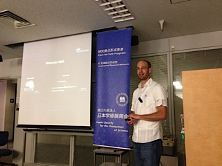
Special Seminar on Diamond Spintronics
July 9, 2013
Keio University Yagami Campus, 14-218 (DR8)
Professor Marko Loncar (Harvard University)
"Quantum optics with NV centers in diamond"
_______________________________
Special seminar on silicon qubit
Time: 2:45 pm, Wednesday, June 5, 2013
Discussion Room 3, building 14 (Sosokan),Keio University
Speaker: Professor Mark A. Eriksson , Physics Dept. University of Wisconsin-Madison
Tittle: "Experimental Progress towards the Hybrid Quantum Dot Silicon Qubit"
_______________________________
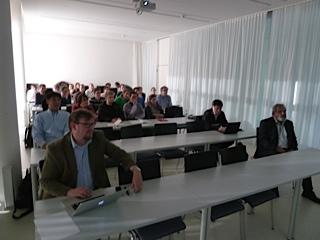
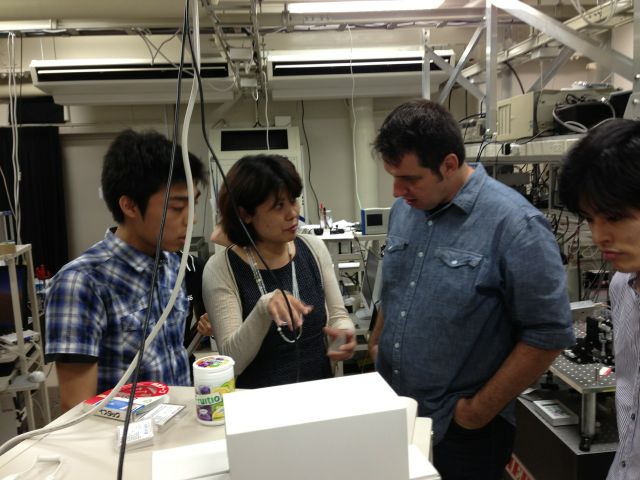
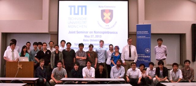
Keio-TU Munchen joint seminar on nanospintronics
Monday, May 27, 2013, 12:30pm-5:30pm
Keio University Yagami Campus, Koseto, Daikaigishitsu
 大阪大学
大阪大学 東京大学
東京大学